DESIGN SERVICE
01
Overview
Socle offers a comprehensive and adaptable model that allows customers to hand off projects starting from the specification definition or GDSII. Socle has the capability to take over the entire design flow and manage it through mass production. Socle has been delivering ASIC design services from legacy to advanced 5nm FinFET processes, collaborating with the numerous foundry partners. Customers have the flexibility to implement cutting-edge process technologies as well as cost-efficient solutions tailored to different applications. Backed by our extensive global network of partners, Socle guarantees the most efficient solutions tailored to all assembly, testing, and logistics needs. Socle stands as your reliable companion in SoC/ASIC development and production services.
SoC / aSIC One-Stop-Shop
")
02
SoC / ASIC Design Service and Verification
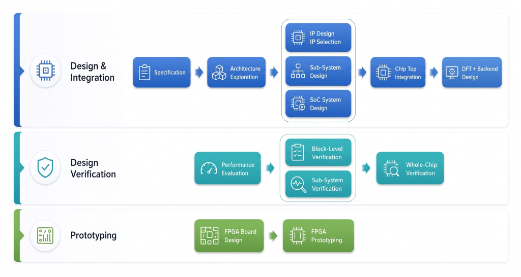
Socle serves as your comprehensive partner for SoC/ASIC development, encompassing everything from initial specification, design and verification to mass production. With the experienced engineer team, Socle collaborate with customers to design their products based on a variety of architectures which includes ARM and RISC-V platform for a large range of applications.
As the complexity of chip design grows, it requires various techniques and a wide range of domain know-how to increase the confidence level of tape-out. Socle provides numerous techniques that are employed to accomplish comprehensive verification closure.
FPGA-based prototyping and emulation solutions facilitate the verification of intricate ASICs, SoCs, systems, and software, thereby expediting the system development process. With extensive experience in FPGA prototype design services, Socle helps our customers to verify the design and develop the related software in advance.
As an independent fabless Design Service, Socle has established partnerships with numerous foundries to help you select an appropriate process technology for your products. Our extensive global partners guarantee the most effective solution for all assembly, testing, and logistics requirements. Socle is your trusted partner for SoC/ASIC development and mass production.
03
IP Offering
We do have a wide variety of independent IP vendors to support Socle’s IP Eco-System for your IP needs of products. With over 500 SoC projects experiences, we could collaborate with customers on methods, technology adoption, and the design process, to implement your idea to productivity and reduce risks.
Our comprehensive IP portfolio provides customization capabilities services with our Eco-Systems IP partners which enhances the rapid emerging technology and interfaces adoption that reduces time-to-market and SoC development risk while ensuring compliance to the respective standards.
In collaboration with leading IP vendors, Socle provides the most state-of-the-art IP portfolio. The ecosystem builds, validates, and delivers the comprehensive IP solution to ensure IP quality, integration and testability, which enables shorter design cycle time, higher first silicon success, and faster time-to-market.


04
Design Implementation
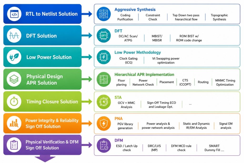
Socle has been delivering SoC design services (SoC-ImP®) by robust flow cover 0.25um to 7nm technology. SoC-ImP® methodology resolves the challenges of million gates by DFT, Power analysis, Placement & Routing, RC Extraction, Timing Analysis, IR Drop / Electro Migration, Design For Manufacturing (DFM), by time to market requirements.
SoC-ImP® flow proven by tablet, IP Cam, 8K TV Set-Top-Box, 5G, AI application…,ect. Over 500 projects
Design Implementation Items
– RTL-to-GDSII, Netlist-to-GDSII, Spec-to-GDSII
– Scan, ATPG, Memory BIST, Boundary Scan
– ARM Processors / RISC-V CPU Configuration/Hardening
– Digital IP hardening
– Hard IP (GDSII) merge
Design Methodology
In Design-For-Testability (DFT) services, Socle delivers scan, boundary scan, memory BIST insertion, and compression, fault coverage analysis services.
In Low power technique, SoC-ImP® integrate low power format (IEEE 1801/UPF/CPF), optimize DVFS (Dynamic Voltage Frequency Scaling), make leakage power saving up to 10X, dynamic power saving up to 20%. And also support clock gated design and Vt cell swap low power methodology.
In timing closure with MMMC (Multi Mode Multi Corner), and on chip variation (OCV) for multiple power domain/on-off domain verification.

Low Power Solution
01 Multi-Vt Cell Swapping
To make customer achieve low power design, Socle delivers Multi-Vt Cell Swapping, PMK (Power Management Kit) insertion, ICG (Isolation Clock Gating) insertion, MSMV (Multi-Supply, Multi-Voltage) design, and Static / Dynamic power analysis.

02 PMK Cell Insertion
PMK : Power Managements Kit
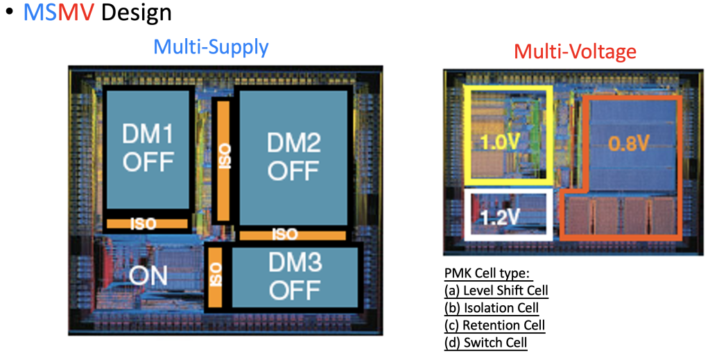

Level Shift Cell : A level shifter cell used by different voltage level (VDDI & VDD)

Isolation Cell : Dedicated isolation cells with one power port. Isolation control will connect to port EN


Retention Cell : State Retention cells with a single retention control port
03 ICG Cell Insertion
ICG (Isolation Clock Gating) : Power saving mechanism. When the circuit is idle mode, ICG are used to turn off part of the DFF clock, make the CLK no need to be toggled all the time
ICG cell consists of Latch, And, Not gate

04 MSMV- Low-Power Equivalence Checking
Define Analysis Style
Set low power option -analysis_style [pre_sim| pre_syn | post_syn | pre_route | post_route]
PRE_sim (by Customer)
– RTL design
– Ready for simulation
– Check syntax and quality for IEEE 1801/UPF/CPF
PRE_syn (by Customer)
– Before gate synthesis
– Check quality for IEEE 1801 / UPF / CPF specification and library
POST_syn
– Logical netlist with isolation, level shifter and retention cells
– Logical netlist without PG connectivity
PRE_route
– Before place and route
– Check quality for IEEE 1801 / UPF / CPF specification and library
– Physical netlist with PG connection
– Power switch related check
POST_route
– Physical netlist with PG connection
– Check a post place and route netlist with inserted isolation, level shifter, state retention, power switch cells, and power / ground connectivity
05 Static / Dynamic Power Analysis
Purpose: Evaluation of the Power Consumption
Static Power (average condition) :
– Customer provide toggle rate (Vector less)
Dynamic Power (real condition) :
– Customer provide VCD (Value Change Dump) file (Vector Based)
Tool : Synopsys PrimeTime PX
Design For Testability
Design For Testability (DFT) consists of IC design techniques that add testability features to a hardware product design. The added features make it easier to develop and apply manufacturing tests to the designed hardware. The purpose of manufacturing tests is to validate the product hardware contains no manufacturing defects, which could adversely affect the product functionality.
01 Boundary Scan Design
For boundary scan design, customer need to prepare a dedicate TDO (Test Data Output) port implement, use Bidirectional PAD by TDO port, number of signals NOT insert boundary scan cell, and deliver Socle if functional signals shared with Boundary Scan signals (TDI, TMS, TCK, TRST)
Below is boundary scan design overview and signal description :
Boundary Scan Design Overview
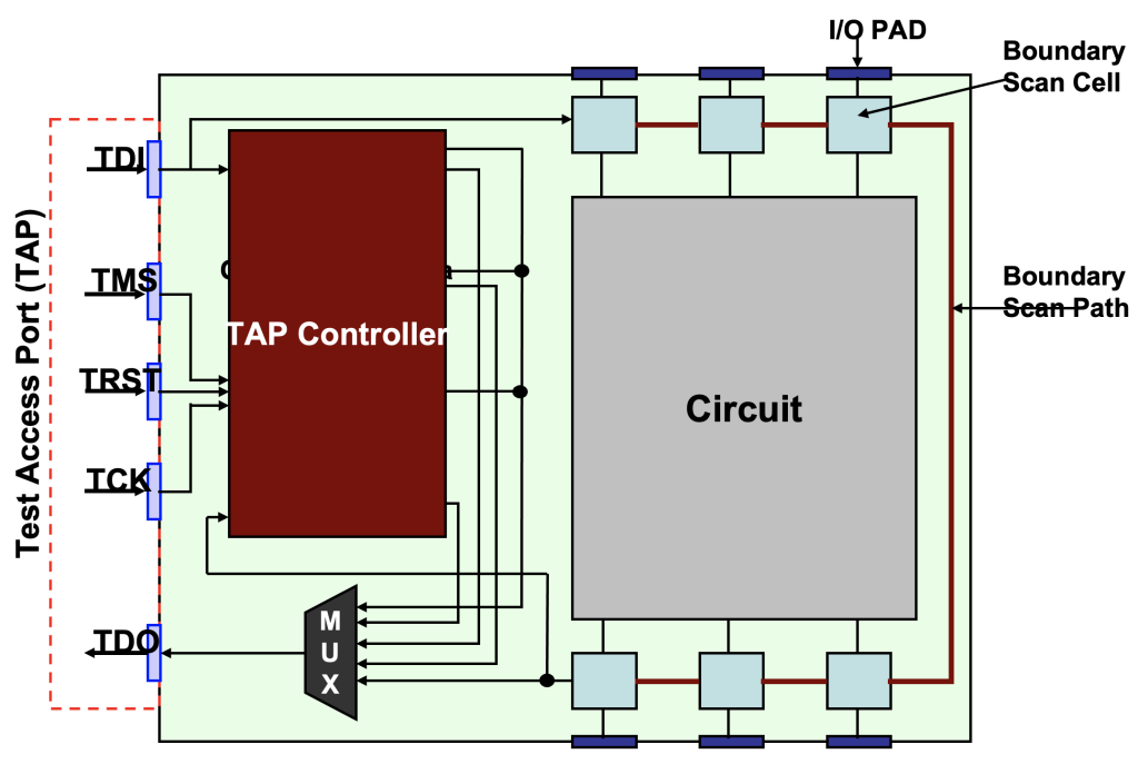
Boundary Scan Signal Description

02 Scan Design
For scan design, customer need to reply below questions :
– How many clocks by the design ?
– Any internally generated clocks ?
– Any internally generated asynchronous sets / resets ?
– Any tri-state buses ?
– How many bi-directional ports by the design ?
– Will scan signals be shared with functional signals ?
– How to bypass PLL & memories ?
– How many scan chains are suitable for the design ?
– Any testing time & power issues ?
Below is scan chain expample and signal description :
Scan chain count :
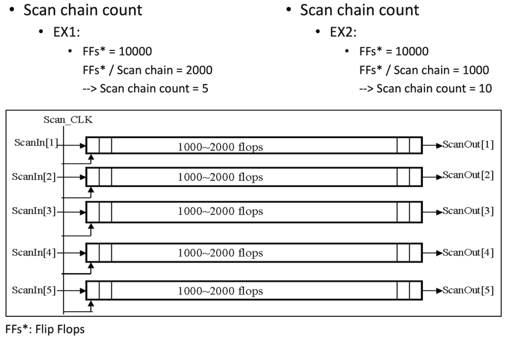
Scan Signal Description

03 MBIST Design
For MBIST design, customer need to provide number of memories by the design, number of memory controllers by the design, at-function-speed or low speed is necessary, with testing time & power issues or not, and deliver Socle if functional signals shared with MBIST signals.
Below is MBIST design overview and signal description :
MBIST Control Overview
For MBIST design, customer need to provide number of memories by the design, number of memory controllers by the design, at-function-speed or low speed is necessary, with testing time & power issues or not, and deliver Socle if functional signals shared with MBIST signals.
Below is MBIST design overview and signal description :
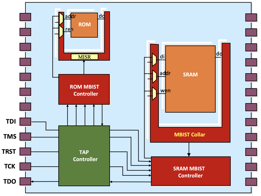
MBIST Signal Description

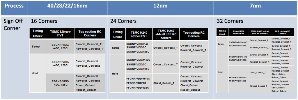
Timing Closure
Timing closure with MMMC (Multi Mode Multi Corner) and on chip variation (OCV) for multiple power domain / on-off domain verification. Socle follow TSMC Recommend Sign Off Corners by difference process node.
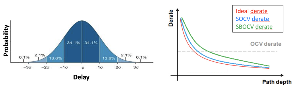
Introduction to OCV
OCV : On Chip Variation
Intrinsic variability of semiconductor process, which impact logic timing
SBOCV : Stage Best OCV
SBOCV provide logic depth and / or cell, net location these derate values, to determine how much impacted by the process variation, by specific path design
SOCV : Statistical OCV
SOCV is Gaussian distribution, the nominal delay (µ), and standard deviation (σ) Each cell delay with the highest probability by +/-3σ interval (3 sigma, up to 99.7%)
SOCV variation characterization
– Variation not path based
– Delay = µ + n*σ (µ: Nominal delay; σ: Standard deviation)
– SOCV used LVF file (Liberty Variation Format)
– SOCV consider Gaussian distribution analysis, could be closer ideal derate
OCV type in TSMC process
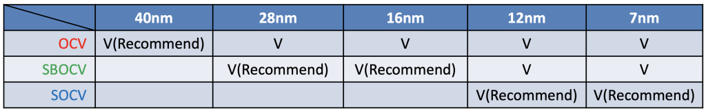
TSMC Recommend Sign Off Corners
– By each mode (Function, DFT) sign off corners